Semiconductor Devices: Difference between revisions
Michaeleden (talk | contribs) |
Idumitriu3 (talk | contribs) |
||
| (35 intermediate revisions by 4 users not shown) | |||
| Line 1: | Line 1: | ||
Last edited by Irene Dumitriu (Spring 2024) | |||
===What are Semiconductors?=== | |||
Semiconductor devices are electronic components with the electronic properties of semiconductors. Silicon, germanium, gallium arsenide, organic semiconductors are among the most common semiconductors used in these devices. | |||
Semiconductor devices are electronic components with the electronic properties of semiconductors. Silicon, germanium, gallium arsenide, organic semiconductors are among the most common semiconductors used in these devices. Semiconductors are materials that are neither good conductors or good insulators. They have a good conductivity between conductors (these tend to be metals) and nonconductors (these insulators tend to be ceramics). Semiconductors do not have to originate organically - the most common semiconductor material are pure elements such as silicon and germanium, but impurities are often added to control the conductivity levels. This process is called doping. The doped semiconductors are called extrinsic semiconductors while pure, impurity-free semiconductors are called intrinsic semiconductors. Intrinsic semiconductors are less conductive than metals as they have a lower amount of charge carriers, or electrons or holes, that can move across the band gap. Extrinsic semiconductors can have higher or lower conductivity depending on the doping. | |||
The conductivity of these semiconductors can also be impacted by environmental changes such as temperature changes. Electrical conductivity depends on two factors: charge-carrier mobility and the concentration of mobile charge carriers. Charge carriers are free electrons or holes that are able to move freely throughout a material, and their mobility is the speed at which these electrons move in a certain direction under the application of a voltage. The free electrons are responsible for determining a current as a current is defined as the rate of electrons flowing through a material in a unit of time. In semiconductors, the charge carrier mobility is negligible as the temperature directly impacts mainly the charge carrier concentration. The band gap theory helps explain how charge carriers move in semiconductors. Unlike metals, semiconductors have a gap between the conduction band and the valence band where the electrons sit without excitation. As temperature increases, these electrons gain energy until they have enough energy to cross the band gap and into the conduction band, decreasing resistivity and increasing conductivity. This behavior is observed mainly in intrinsic semiconductors. In extrinsic semiconductors, the type of doping can affect the conductivity negatively or positively. | |||
Due to low cost, reliability, ability to control conductivity, and compactness, semiconductors are used for a wide range of applications. They also have a wide range of current and voltage handling capabilities, contributing to their suitability for a number of operations. They are commonly found in power devices, optical sensors, and light emitters. Perhaps more importantly, they are readily integrated into microelectronic uses as key elements for the majority of electronic systems, including communications, consumer, data-processing, and industrial-control equipment. | |||
[[File:Intelthing.jpg|frame|border|right|A raw board with many transistors in it!]] | [[File:Intelthing.jpg|frame|border|right|A raw board with many transistors in it!]] | ||
| Line 14: | Line 19: | ||
==The Main Idea== | ==The Main Idea== | ||
The | Semiconductors work by using the electric properties of the p-n junction that makes up a diode. The junction is formed through a process called doping. Doping involves turning silicon into a conductor by changing the behavior of its electrons. In n-type doping, a phosphorus/arsenic impurity is introduced so that the valence will have free electrons to allow a electric current to flow. Since extra electrons are negative in charge, this type of doping is called n-type doping referred to by "n" in the p-n junction. In the p-type doping, a boron/gallium impurity is introduced to the silicon lattice so the valence will have an empty electron orbital. Because the empty area implies the absence of an electron and thus creates a positive charge, "p" was assigned as the name of the doping type. | ||
[[File:n-type.gif|frame|border|right|N-Type Material]] | |||
[[File: | [[File:p-type.png|frame|none|left|P-Type Material]] | ||
The two most useful forms of semiconductor devices are diodes and transistors. Diodes are the simplest semiconductor device, which conducts current easily in one direction but conducts almost no current in the other direction. These are made by joining two pieces of semiconducting material, a junction called a "p-n" junction. One of the pieces contains a small amount of boron and the other contains a small amount of phosphorus. Transistors are constructed through two semiconducting junctions, or "p-n" junctions. These are the most common elements in digital circuits. The conductivity of these semiconductors can be controlled by introduction of an electric or magnetic field, by exposure to light or heat, or by mechanical deformation of a doped monocrystalline grid. Due to this, semiconductors are extremely useful and can be altered to fit specific purposes. | |||
=== | ===Semiconductors & Applications in Solid-State Physics=== | ||
The key principle that is often used in solid-state physics is the carrier effective mass. This refers to the mass a particle (within the semiconductor) seems to have when interacting with other identical particles in a thermal distribution. This constant is simplified version of the band theory and influences measurable properties of a solid, including the efficiency of the devices that semiconductors are used in for example, solar cell efficiency and integrated circuit speed. So, how do we actually measure the carrier effective masses in a semiconductor? | |||
Large parts of the simplicity of the free electron gas model can be saved by assigning effective masses to the carriers. Only electrons and holes at the band edges (characterized by a wave vector kex) participate in the generation - recombination process that is the hallmark of semiconductors. A particle's effective mass is the mass that it seems to have when responding to forces, or the mass that it seems to have when interacting with other identical particles in a thermal distribution. One of the results from the band theory of solids is that the movement of particles over long distances can be very different from their motion in a vacuum. The effective mass is a quantity that is used to simplify band structures by modeling the behavior of a free particle with that mass. Sometimes the effective mass can be considered to be a simple constant of a material, however, the value of effective mass depends on the purpose for which it is used, and can vary depending on a number of factors. For electrons or electron holes in a solid, the effective mass is usually stated in units of the rest mass of an electron, me (9.11×10⁻³¹ kg). In these units it is usually in the range 0.01 to 10, but can also be lower or higher—for example, reaching 1,000 in exotic heavy fermion materials, or anywhere from zero to infinity (depending on definition) in graphene. The effective mass of a semiconductor is obtained by fitting the actual electron diagram around the conduction band minimum or the valence band maximum by a parabola - this is called an E-K diagram (shown below). It shows the relationship between the energy and momentum of available quantum mechanical states for electrons in the material. As it simplifies the more general band theory, the electronic effective mass can be seen as an important basic parameter that influences measurable properties of a solid, including everything from the efficiency of a solar cell to the speed of an integrated circuit. | |||
[[File:IMG 2424.jpg|Diagram of an EK diagram|350 px|]] | |||
[[File: | |||
===Detecting Doping=== | |||
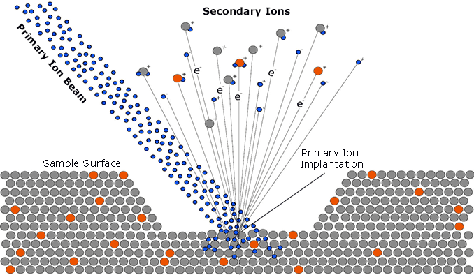
Secondary ion mass spectroscopy (SIMS) is a very powerful technique for the analysis of impurities in solids. SIMS can be utilized for semiconductor dopant profiling. The technique relies on removal of material from a solid by sputtering and on analysis of the sputtered ionized species; all elements are detected. SIMS can detect dopant densities as low as 10^14 cm^-3. The dopant density profile that is generated is based on the ion signal versus time plot. The time axis is converted to a depth axis by measuring the depth of the crater at the end of the measurement assuming a constant sputtering rate. For example, boron is implanted into silicon at a given energy and dose to create a standard. The secondary ion signal is calibrated by assuming the total amount of boron in the sample to equal to the implanted boron. The unknown sample of B implanted into silicon is then compared to the standard. However, there is limited dynamic range of the SIMS instrument that can contribute to slightly deeper junctions and discrepancies in the lowly doped portions of the profile. When sputtering from a highly doped region to a lowly doped region, the crater walls still contain the entire doping density profile. SIMS also measures total dopant density, regardless of activation. Thus going back to the silicon-boron example, the dopant profile shows dependence of electrical activation of boron implanted into silicon on implant dose and activation temperature. | |||
[[File:Sims-technique-schematic.png|frame|none|left|Example of SIMS]] | |||
===Determining Semiconductor Resistivity and Conductivity=== | |||
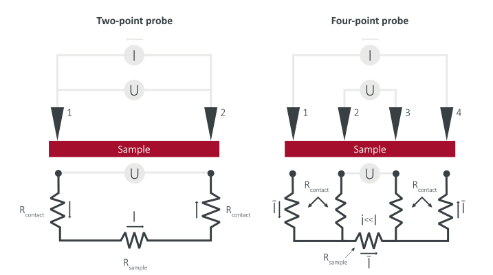
== | Methods for determining the resistivity and conductivity of material involve galvanostatic or potentiostatic tests. In a galvanostatic test, a constant current is applied and the voltage is measured. In a potentiostatic test, a constant voltage is applied and the current is measured. An electrochemical analyzer can be used with either a 2-point or 4-point method. With the 2-point method, there can be contact resistance between the material and the wires, falsely increasing the resistivity. The 4-point technique overcomes this issue by using four wires. A current is conducted and measured through the endpoints of the bar while two wires are connected to the inner points of the bar so that they can measure the voltage produced across the inner bar. Once the data is collected, Ohm’s law can be used to calculate the resistance where the resistance is 1/slope of the current vs. voltage graph. Resistivity is | ||
<math> | |||
𝜌 = R \ {\frac{A}{L}} | |||
</math>, where R is the resistance, A is the cross-sectional area, and L is the length. Conductivity is | |||
<math> | |||
𝜎 = 𝜌^{-1} | |||
</math>. | |||
[[File:2pp_vs_4pp_resistivity.png|frame|border|center|The 2-point method vs. the 4-point method in determining the resistivity of sample.]] | |||
= | However, this method only works for bulk materials. If the semiconductor is in the form of a thin film, then a 4-point colinear probe can be used instead. The method works by measuring the resistance of the material by applying a current through the two outer probes and measuring the voltage of the two inner probes. The resistivity and conductivity calculations are more complicated for thin films as correction factors need to be applied in order to adjust the data for the film thickness, the probe's placement, and other factors. For example, a correction factor needs to be used when the thickness is less than or equal to half the probe spacing. If this is true, then the resistivity is | ||
<math> | |||
𝜌 = (R)\ (2𝜋)\ (s)\ (F1) | |||
</math> where s is the spacing and F1 is the correction factor. | |||
===A Mathematical Model=== | |||
== | Semiconductors operate based on the concept of thermal energy exciting electrons and causing them to jump to the next higher (unoccupied) energy band. | ||
These electrons can pick up energy (and drift speed) from an applied electric field. The filled energy band is called the “valence” band, and the nearly unoccupied higher energy band is called the “conduction” band. The number of electrons excited into the conduction band is proportional to a value called the Boltzmann constant, equivalent to the value: | |||
<math> | |||
e^{-E_{\text{gap}} / k_B T} | |||
</math>. | |||
Therefore, high conductivity (corrosponding to a favorable Boltzmann factor) can be calculated according to | |||
<math> | |||
T = 2 \pi \sqrt{\frac{m}{k}} | |||
</math>, | |||
where <math>m</math> is the mass of the object in kilograms, <math>k</math> is the spring constant, and <math>T</math> is the period of oscillation in seconds. In addition, the total conventional current in a semiconductor can be calculated, according to the equation | |||
<math> | |||
I = e n_n A u_n E + e n_p A u_p E | |||
</math>. | |||
===A Conceptual Model=== | |||
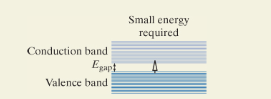
The following diagram demonstrates how electron excitement in semiconductors works. Semiconductors are materials with small band gaps between the valence band and conduction bands. As you can see, a small amount of thermal energy is needed to promote an electron to the conduction band in a semiconductor. | |||
A | [[File:conceptual.png|frame|none|left|A Conceptual Model of the Semiconductor]] | ||
===A Computational Model=== | |||
[https://phet.colorado.edu/sims/cheerpj/semiconductor/latest/semiconductor.html?simulation=semiconductor Semiconductor Simulation] | |||
==History== | ==History== | ||
| Line 76: | Line 96: | ||
Russell Ohl discovers the p-n junction. | Russell Ohl discovers the p-n junction. | ||
'''1940s''' | |||
Semiconductors were used only as two-terminal devices, such as rectifiers and photodiodes. They were most commonly used as detectors in radios, through devices called "cat's whiskers". During the era of WWII, researchers worked with semiconductors and cat's whiskers to make more effective diodes. | |||
''' | '''1947''' | ||
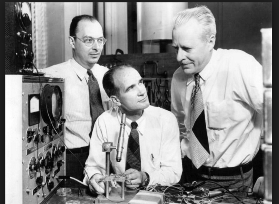
William Shockley and John Bardeen worked together to create a triode-like semiconductor: the first transistor. They realized that if there were some way to control the flow of the electrons from the emitter to the collector of this newly discovered diode, an amplifier could be built.The first transistor was officially created on the 23rd of December, 1947. | |||
'''1956''' | |||
John Bardeen, William Shockley, and another researcher named Walter Houser Brattain were credited for the invention and awarded a Nobel Prize for physics in 1956 for their work. After this, the utilization of semiconductors soon advanced to even more complicated applications. | |||
'''1960s''' | |||
In the late 1960s, transistors moved from being germanium based to silicon based. Gordon K Teal was most responsible for this advancement, and his company, Texas Instruments, profited greatly. Portable radios are just one popular invention that benefited from silicon based semiconductors. Now, silicon based semiconductors constitute more than 95 percent of all semiconductor hardware sold worldwide. | |||
'''1970s''' | '''1970s''' | ||
Silicon technology is modernized and the race to fit all semiconductor processor technology into one chip is most active. | Silicon technology is modernized and the race to fit all semiconductor processor technology into one chip is most active. | ||
[[File:chip.jpg]] | '''2000''' | ||
Nobel Prize in physics awarded to Zhores I. Alferov and Herbert Kroemer for developing semiconductor heterostructures used in high-speed- and opto-electronics and half to Jack S. Kilby "for his part in the invention of the integrated circuit." | |||
[[File:transistorwork.png|frame|none|none|John Bardeen, William Shockley, and Walter Houser Brattain, winners of the Nobel Prize for their invention of the transistor, are pictured above.]] | |||
===Connectedness=== | |||
Semiconductors are crucial to modern technology, and are used for memory storage as well as so many other technological innovations. This technology is used every day by millions of people for thousands of different applications. Most people in the world have used semiconductors in one way or another, even if they weren't aware of it. It is specifically connected to the major of Biomedical Engineering through memory storage and the complex computer programs used every day to conduct business and create simulations for the furthering of biomedical research. All industrial applications of semiconductors are very applicable, from amplifiers to transistors to silicon disks. Without semiconductors, much of the technology that the general population relies on today would not be possible. | |||
Semiconductors are used in essentially every part of this technological and electronically-dependent world we live in today. They have both conductor and insulator properties and includes all of the metal we see in wires. Computers, phones, and other electronic devices all use semiconductors to fulfill their functions such as communication and efficiency. The most important aspect of semiconductors is utilization, which is shown through the use of switches. Inside electronic devices, the switches exist in extremely large numbers, which is why electronic devices process information in an incredible speed with surprising efficiency. | |||
Semiconductors are connected to chemical engineering largely through their industrial creation. The process of depositing each layer of material onto the wafer is a chemical process controlled by deposition of gaseous metals onto the wafer. There are an incredible variety of steps from material preparation to packaging which can be optimized by an eager chemical engineer. | |||
Another example that was discussed previously on this page is the usage of silicon in photovoltaic devices. Silicon is used because it is the first semiconductor that was commercialized successfully. Many commercial companies are very proficient in making silicon devices, so the silicon is not necessarily used because it is the best material for harnessing the electricity from the photovoltaic effect. The silicon crystals allow the power to reach the external electrical circuit, but the silicon doesn't absorb sunlight as efficiently because it needs to be ten to one hundred times thicker than an advanced thin-film cell. It is also favored because of the low maintenance. A unique oxide forms when silicon is exposed to high temperatures that serves to neutralize defects on the silicon surface. The frontier for replacing the silicon looks quite bleak because of the practicality of manufacturing silicon crystalline semiconductors, but new research is being conducted on using silicon with lower purity or combining it with other semiconductor materials. | |||
==Types of Semiconductors== | |||
===Diodes=== | |||
[[File:Diode_current_wiki.png|314px|thumb|right|top|IV Characteristic of a Diode]] | |||
Diodes are really great! In a simple sense, they can give you a "point of no return" in your circuit (but they can actually do much more than that). | |||
Three interesting things should be observed from the IV characteristic shown to the right: | |||
# For small positive voltages and above, the diode does not limit the current (the line is almost vertical)! | |||
# For small to larger negative voltages, the diode resists current (the line is almost flat). | |||
# For a large negative voltage (the breakdown voltage) the diode gives up (no one is perfect). | |||
We can formally define this line with the Shockley Diode Equation, which formalizes this observation: | |||
<math display="block"> | |||
I = I_S \left( e^{\frac{V_D}{n V_T}} - 1 \right) | |||
</math> where | |||
<math>I</math> is the diode current, | |||
<math>I_S</math> is the reverse bias saturation current (or scale current), | |||
<math>V_D</math> is the voltage across the diode, | |||
<math>V_T</math> is the thermal voltage, and | |||
<math>n</math> is the ideality factor, (1 if the diode is ideal, greater than 1 if it is imperfect). | |||
A great practical use for diodes is a rectifier: | |||
[[File:Gratz.rectifier.en.svg|frame|border|center|Diodes groups the positive and negative signals together]] | |||
This makes sure that when a positive voltage appears on either line, it is redirected to a single positive line, and the same for the negatives. | |||
BAM! AC to DC, that's pretty easy, you can charge your phone with that. | |||
In reality a capacitor is added in parallel with the load to try to smooth out the ripples. | |||
A voltage regulator after the rectifying step is also a popular choice, depending on the needs of the application. | |||
Another super useful application is that of a back up power supply: simply connect two supplies in parallel with the positive terminals buffered with diodes. The higher of the two voltages is always used and the transition between supplies is seamless. | |||
===Zener Diodes=== | |||
Some diodes (Zener) are made to have small breakdown voltages. | |||
Since during breakdown the IV curve is almost vertical (it's really an exponential), the current is independent (almost) from voltage. | |||
You can then wire up a Zener diode in reverse to a point in the circuit, and it will accept as much current as it needs to to reach that | |||
breakdown voltage. Because of this a great practical use for Zener diodes is a voltage regulator since the voltage is set when the diode is | |||
manufactured and does not change greatly with a varying power supply. | |||
===Bipolar Junction Transistors=== | |||
[[Image:BJT NPN symbol (case).svg|75px|thumb|NPN BJT]] | |||
[[Image:BJT PNP symbol (case).svg|75px|thumb|PNP BJT]] | |||
Shortly after the invention of the first transistor (which was OK), the BJT landed, which was the first transistor to be prolific in the field. | |||
It was made using two alternating NP junctions as shown below: | |||
[[File:NPN BJT (Planar) Cross-section.svg|frame|border|center|NPN BJT (Planar) Cross-section]] | |||
Really transistors (and by extension all that is needed for a computer to be built) are amplifiers (OK, to build all computers you need an inverting amplifier, but one can be built using the BJT). | |||
If one is used to thinking of them as an electrically-controlled switch, you can simply think of a switch as an amplifier with a gain of <math>\infty</math>. | |||
A simple model of a BJT is a linear current-controlled current source, i.e. the base to emitter (B to E) current <math>I_{BE}</math> is proportional to | |||
the collector to emitter (C to E) current <math>I_{CE}</math>. The proportionality constant <math>\beta</math> can be thought of as the "gain" of the | |||
transistor. This gives a relationship of <math>I_{CE} = \beta I_{BE}</math>. | |||
[[File:Current-Voltage relationship of BJT.png|thumb|right|Current-Voltage relationship of BJT]] | |||
Sadly there is no source of infinite power, so the output to our amplifier tops off when it can't supply any more power. | |||
This can be seen with the graph on the right. | |||
The simple model then only works for the tiny linear part at the start of the graph, even so its not ''that'' linear. | |||
The BJT proved to be power hungry, pretty non-linear and sensitive to the environment (temperature, etc.). | |||
These growing pains lead to a new development, called the MOSFET. | |||
===MOSFETs=== | |||
MOSFETs are the coolest, they are less power-hungy and easier to work with when compared to BJTs. | |||
Instead of having a current control, which uses power and gets the control and the output signal coupled together, | |||
a MOSFET's output is controlled by the electric Field (the F in MOSFET) the control signal creates on one of the plates of the MOSFET. | |||
Since the control signal and the output are electrically disconnected (as you would see in a capacitor) there is much less power draw | |||
from this type of transistor. | |||
We can see how linear this thing is with its IV characteristic: <math>I_D= \mu_n C_{ox}\frac{W}{L} \left( (V_{GS}-V_{th})V_{DS}-\frac{V_{DS}^2}{2} \right)</math> | |||
Apart from the control signal <math>V_{DS}</math> and constants, the voltage across the output portion of the MOSFET is linearly related to the current! | |||
This means that the MOSFET behaves like a voltage controlled resistor, and a resistor is something much easier to analyse and work with. | |||
Most circuits with an enormous amount of transistors these days use primarily MOSFETs. BJTs are still useful for temperature and light sensing | |||
applications. | |||
==Industrial Semiconductor Fabrication== | |||
Semiconductors are mass produced in specialized factories called foundries or fabs. The process consists of multiple chemical and photolithographic steps which add layers to a wafer usually made of silicon. The entire process usually takes around 2 months but it can last up to 4. | |||
The semiconductor product is rated by the size of the chip's process gate length, where processes with smaller gate lengths are typically harder to make. There are 10-20 different sized chips being fabricated around the world as of 2018. There is an immense amount of attention and money being dedicated to improving semiconductor fabrication process efficiency. | |||
[[File:feol.png|frame|none|left|Steps to fabricate a semiconductor device]] | |||
==Examples== | |||
===Simple=== | |||
[[File:Cat'swhiskerdetector.jpg]] | |||
A simple application of a semiconductor would be the Cat's Whisker detector for radios, invented in the early 1900s. | |||
===Moderate=== | |||
[[File:Opticallsensor.jpg]] | |||
Optical sensors are moderately difficult applications of semiconductors. Optical sensors are electronic detectors that convert light into an electronic signal. They are used in many industrial and consumer applications. An example would include lamps that turn on automatically in response to darkness. | |||
===Difficult=== | |||
[[File:Complicated_semiconductor.jpg]] | |||
A very complicated application of a semiconductor is its use in modern cellular phone devices, such as its use here in the iPhone 6. | |||
== See also == | == See also == | ||
| Line 119: | Line 271: | ||
http://www.britannica.com/technology/semiconductor-device | http://www.britannica.com/technology/semiconductor-device | ||
Information about Diodes: | |||
https://en.wikipedia.org/wiki/Diode | |||
Information about BJTs: | |||
https://en.wikipedia.org/wiki/Bipolar_junction_transistor | |||
Information about MOSFETs: | |||
https://en.wikipedia.org/wiki/MOSFET | |||
Semiconductor Device Fabrication | |||
https://en.wikipedia.org/wiki/Semiconductor_device_fabrication | |||
==References== | ==References== | ||
| Line 128: | Line 296: | ||
Huculak, M. (2014, September 19). IPhone 6 and iPhone 6 Plus get teardown by iFixit • The Windows Site for Enthusiasts - Pureinfotech. Retrieved December 3, 2015, from http://pureinfotech.com/2014/09/19/iphone-6-iphone-6-plus-get-teardown-ifixit/ | Huculak, M. (2014, September 19). IPhone 6 and iPhone 6 Plus get teardown by iFixit • The Windows Site for Enthusiasts - Pureinfotech. Retrieved December 3, 2015, from http://pureinfotech.com/2014/09/19/iphone-6-iphone-6-plus-get-teardown-ifixit/ | ||
Introduction to Secondary Ion Mass Spectrometry (SIMS) technique. (n.d.). Retrieved November 15, 2020, from https://www.cameca.com/products/sims/technique | |||
John Bardeen, William Shockley and Walter Brattain at Bell Labs, 1948. (n.d.). Retrieved December 3, 2015, from https://en.wikipedia.org/wiki/John_Bardeen#/media/File:Bardeen_Shockley_Brattain_1948.JPG | John Bardeen, William Shockley and Walter Brattain at Bell Labs, 1948. (n.d.). Retrieved December 3, 2015, from https://en.wikipedia.org/wiki/John_Bardeen#/media/File:Bardeen_Shockley_Brattain_1948.JPG | ||
The Nobel Prize in Physics 1956. NobelPrize.org. Nobel Media AB 2018. Sun. 25 Nov 2018. <https://www.nobelprize.org/prizes/physics/1956/summary/> | |||
The Nobel Prize in Physics 2000. NobelPrize.org. Nobel Media AB 2018. Sun. 25 Nov 2018. <https://www.nobelprize.org/prizes/physics/2000/summary/> | |||
เซ็นเซอร์แสง (Optical Sensor) - Elec-Za.com. (2014, July 28). Retrieved December 3, 2015, from http://www.elec-za.com/เซ็นเซอร์แสง-optical-sensor/ | เซ็นเซอร์แสง (Optical Sensor) - Elec-Za.com. (2014, July 28). Retrieved December 3, 2015, from http://www.elec-za.com/เซ็นเซอร์แสง-optical-sensor/ | ||
Semiconductor device. (2015, November 30). Retrieved December 3, 2015, from https://en.wikipedia.org/wiki/Semiconductor_device | Semiconductor device. (2015, November 30). Retrieved December 3, 2015, from https://en.wikipedia.org/wiki/Semiconductor_device | ||
Semiconductor Fabrication. (25 November 2018). http://www.iue.tuwien.ac.at/phd/rovitto/node10.html | |||
Shah, A. (2013, May 13). Intel loses ground as world's top semiconductor company, survey says. Retrieved December 3, 2015, from http://www.pcworld.com/article/2038645/intel-loses-ground-as-worlds-top-semiconductor-company-survey-says.html | Shah, A. (2013, May 13). Intel loses ground as world's top semiconductor company, survey says. Retrieved December 3, 2015, from http://www.pcworld.com/article/2038645/intel-loses-ground-as-worlds-top-semiconductor-company-survey-says.html | ||
| Line 142: | Line 318: | ||
Sze, S. (1981). Physics of semiconductor devices (2nd ed.). New York: Wiley. | Sze, S. (1981). Physics of semiconductor devices (2nd ed.). New York: Wiley. | ||
"Timeline." Timeline | The Silicon Engine | Computer History Museum. The Silicon Engine, n.d. Web. 27 Nov. 2016. | "Timeline." Timeline | The Silicon Engine | Computer History Museum. The Silicon Engine, n.d. Web. 27 Nov. 2016. | ||
[[Category:Simple Circuits]] | [[Category:Simple Circuits]] | ||
Latest revision as of 22:30, 14 April 2024
Last edited by Irene Dumitriu (Spring 2024)
What are Semiconductors?
Semiconductor devices are electronic components with the electronic properties of semiconductors. Silicon, germanium, gallium arsenide, organic semiconductors are among the most common semiconductors used in these devices. Semiconductors are materials that are neither good conductors or good insulators. They have a good conductivity between conductors (these tend to be metals) and nonconductors (these insulators tend to be ceramics). Semiconductors do not have to originate organically - the most common semiconductor material are pure elements such as silicon and germanium, but impurities are often added to control the conductivity levels. This process is called doping. The doped semiconductors are called extrinsic semiconductors while pure, impurity-free semiconductors are called intrinsic semiconductors. Intrinsic semiconductors are less conductive than metals as they have a lower amount of charge carriers, or electrons or holes, that can move across the band gap. Extrinsic semiconductors can have higher or lower conductivity depending on the doping.
The conductivity of these semiconductors can also be impacted by environmental changes such as temperature changes. Electrical conductivity depends on two factors: charge-carrier mobility and the concentration of mobile charge carriers. Charge carriers are free electrons or holes that are able to move freely throughout a material, and their mobility is the speed at which these electrons move in a certain direction under the application of a voltage. The free electrons are responsible for determining a current as a current is defined as the rate of electrons flowing through a material in a unit of time. In semiconductors, the charge carrier mobility is negligible as the temperature directly impacts mainly the charge carrier concentration. The band gap theory helps explain how charge carriers move in semiconductors. Unlike metals, semiconductors have a gap between the conduction band and the valence band where the electrons sit without excitation. As temperature increases, these electrons gain energy until they have enough energy to cross the band gap and into the conduction band, decreasing resistivity and increasing conductivity. This behavior is observed mainly in intrinsic semiconductors. In extrinsic semiconductors, the type of doping can affect the conductivity negatively or positively.
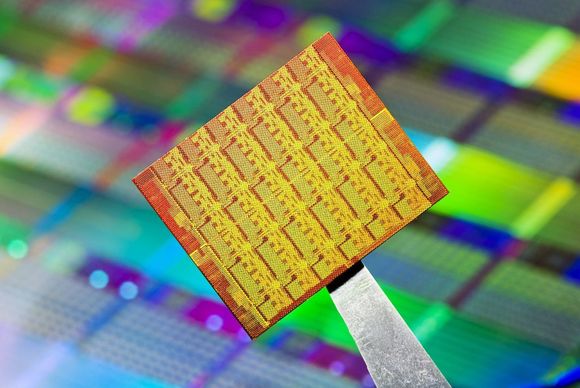
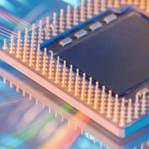
Due to low cost, reliability, ability to control conductivity, and compactness, semiconductors are used for a wide range of applications. They also have a wide range of current and voltage handling capabilities, contributing to their suitability for a number of operations. They are commonly found in power devices, optical sensors, and light emitters. Perhaps more importantly, they are readily integrated into microelectronic uses as key elements for the majority of electronic systems, including communications, consumer, data-processing, and industrial-control equipment.
The Main Idea
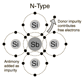
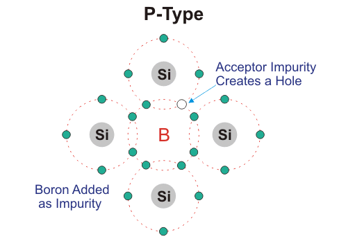
Semiconductors work by using the electric properties of the p-n junction that makes up a diode. The junction is formed through a process called doping. Doping involves turning silicon into a conductor by changing the behavior of its electrons. In n-type doping, a phosphorus/arsenic impurity is introduced so that the valence will have free electrons to allow a electric current to flow. Since extra electrons are negative in charge, this type of doping is called n-type doping referred to by "n" in the p-n junction. In the p-type doping, a boron/gallium impurity is introduced to the silicon lattice so the valence will have an empty electron orbital. Because the empty area implies the absence of an electron and thus creates a positive charge, "p" was assigned as the name of the doping type.
The two most useful forms of semiconductor devices are diodes and transistors. Diodes are the simplest semiconductor device, which conducts current easily in one direction but conducts almost no current in the other direction. These are made by joining two pieces of semiconducting material, a junction called a "p-n" junction. One of the pieces contains a small amount of boron and the other contains a small amount of phosphorus. Transistors are constructed through two semiconducting junctions, or "p-n" junctions. These are the most common elements in digital circuits. The conductivity of these semiconductors can be controlled by introduction of an electric or magnetic field, by exposure to light or heat, or by mechanical deformation of a doped monocrystalline grid. Due to this, semiconductors are extremely useful and can be altered to fit specific purposes.
Semiconductors & Applications in Solid-State Physics
The key principle that is often used in solid-state physics is the carrier effective mass. This refers to the mass a particle (within the semiconductor) seems to have when interacting with other identical particles in a thermal distribution. This constant is simplified version of the band theory and influences measurable properties of a solid, including the efficiency of the devices that semiconductors are used in for example, solar cell efficiency and integrated circuit speed. So, how do we actually measure the carrier effective masses in a semiconductor?
Large parts of the simplicity of the free electron gas model can be saved by assigning effective masses to the carriers. Only electrons and holes at the band edges (characterized by a wave vector kex) participate in the generation - recombination process that is the hallmark of semiconductors. A particle's effective mass is the mass that it seems to have when responding to forces, or the mass that it seems to have when interacting with other identical particles in a thermal distribution. One of the results from the band theory of solids is that the movement of particles over long distances can be very different from their motion in a vacuum. The effective mass is a quantity that is used to simplify band structures by modeling the behavior of a free particle with that mass. Sometimes the effective mass can be considered to be a simple constant of a material, however, the value of effective mass depends on the purpose for which it is used, and can vary depending on a number of factors. For electrons or electron holes in a solid, the effective mass is usually stated in units of the rest mass of an electron, me (9.11×10⁻³¹ kg). In these units it is usually in the range 0.01 to 10, but can also be lower or higher—for example, reaching 1,000 in exotic heavy fermion materials, or anywhere from zero to infinity (depending on definition) in graphene. The effective mass of a semiconductor is obtained by fitting the actual electron diagram around the conduction band minimum or the valence band maximum by a parabola - this is called an E-K diagram (shown below). It shows the relationship between the energy and momentum of available quantum mechanical states for electrons in the material. As it simplifies the more general band theory, the electronic effective mass can be seen as an important basic parameter that influences measurable properties of a solid, including everything from the efficiency of a solar cell to the speed of an integrated circuit.
Detecting Doping
Secondary ion mass spectroscopy (SIMS) is a very powerful technique for the analysis of impurities in solids. SIMS can be utilized for semiconductor dopant profiling. The technique relies on removal of material from a solid by sputtering and on analysis of the sputtered ionized species; all elements are detected. SIMS can detect dopant densities as low as 10^14 cm^-3. The dopant density profile that is generated is based on the ion signal versus time plot. The time axis is converted to a depth axis by measuring the depth of the crater at the end of the measurement assuming a constant sputtering rate. For example, boron is implanted into silicon at a given energy and dose to create a standard. The secondary ion signal is calibrated by assuming the total amount of boron in the sample to equal to the implanted boron. The unknown sample of B implanted into silicon is then compared to the standard. However, there is limited dynamic range of the SIMS instrument that can contribute to slightly deeper junctions and discrepancies in the lowly doped portions of the profile. When sputtering from a highly doped region to a lowly doped region, the crater walls still contain the entire doping density profile. SIMS also measures total dopant density, regardless of activation. Thus going back to the silicon-boron example, the dopant profile shows dependence of electrical activation of boron implanted into silicon on implant dose and activation temperature.
Determining Semiconductor Resistivity and Conductivity
Methods for determining the resistivity and conductivity of material involve galvanostatic or potentiostatic tests. In a galvanostatic test, a constant current is applied and the voltage is measured. In a potentiostatic test, a constant voltage is applied and the current is measured. An electrochemical analyzer can be used with either a 2-point or 4-point method. With the 2-point method, there can be contact resistance between the material and the wires, falsely increasing the resistivity. The 4-point technique overcomes this issue by using four wires. A current is conducted and measured through the endpoints of the bar while two wires are connected to the inner points of the bar so that they can measure the voltage produced across the inner bar. Once the data is collected, Ohm’s law can be used to calculate the resistance where the resistance is 1/slope of the current vs. voltage graph. Resistivity is [math]\displaystyle{ 𝜌 = R \ {\frac{A}{L}} }[/math], where R is the resistance, A is the cross-sectional area, and L is the length. Conductivity is [math]\displaystyle{ 𝜎 = 𝜌^{-1} }[/math].
However, this method only works for bulk materials. If the semiconductor is in the form of a thin film, then a 4-point colinear probe can be used instead. The method works by measuring the resistance of the material by applying a current through the two outer probes and measuring the voltage of the two inner probes. The resistivity and conductivity calculations are more complicated for thin films as correction factors need to be applied in order to adjust the data for the film thickness, the probe's placement, and other factors. For example, a correction factor needs to be used when the thickness is less than or equal to half the probe spacing. If this is true, then the resistivity is [math]\displaystyle{ 𝜌 = (R)\ (2𝜋)\ (s)\ (F1) }[/math] where s is the spacing and F1 is the correction factor.
A Mathematical Model
Semiconductors operate based on the concept of thermal energy exciting electrons and causing them to jump to the next higher (unoccupied) energy band. These electrons can pick up energy (and drift speed) from an applied electric field. The filled energy band is called the “valence” band, and the nearly unoccupied higher energy band is called the “conduction” band. The number of electrons excited into the conduction band is proportional to a value called the Boltzmann constant, equivalent to the value: [math]\displaystyle{ e^{-E_{\text{gap}} / k_B T} }[/math]. Therefore, high conductivity (corrosponding to a favorable Boltzmann factor) can be calculated according to [math]\displaystyle{ T = 2 \pi \sqrt{\frac{m}{k}} }[/math], where [math]\displaystyle{ m }[/math] is the mass of the object in kilograms, [math]\displaystyle{ k }[/math] is the spring constant, and [math]\displaystyle{ T }[/math] is the period of oscillation in seconds. In addition, the total conventional current in a semiconductor can be calculated, according to the equation [math]\displaystyle{ I = e n_n A u_n E + e n_p A u_p E }[/math].
A Conceptual Model
The following diagram demonstrates how electron excitement in semiconductors works. Semiconductors are materials with small band gaps between the valence band and conduction bands. As you can see, a small amount of thermal energy is needed to promote an electron to the conduction band in a semiconductor.
A Computational Model
History
1874 Ferdinand Braun discovers that current flows freely in only one direction when a metal point and a galena crystal are put together.
1901 Jagadis Bose takes ownership of the discovery of the semiconductor crystal for detecting radio waves.
1940 Russell Ohl discovers the p-n junction.
1940s Semiconductors were used only as two-terminal devices, such as rectifiers and photodiodes. They were most commonly used as detectors in radios, through devices called "cat's whiskers". During the era of WWII, researchers worked with semiconductors and cat's whiskers to make more effective diodes.
1947 William Shockley and John Bardeen worked together to create a triode-like semiconductor: the first transistor. They realized that if there were some way to control the flow of the electrons from the emitter to the collector of this newly discovered diode, an amplifier could be built.The first transistor was officially created on the 23rd of December, 1947.
1956 John Bardeen, William Shockley, and another researcher named Walter Houser Brattain were credited for the invention and awarded a Nobel Prize for physics in 1956 for their work. After this, the utilization of semiconductors soon advanced to even more complicated applications.
1960s In the late 1960s, transistors moved from being germanium based to silicon based. Gordon K Teal was most responsible for this advancement, and his company, Texas Instruments, profited greatly. Portable radios are just one popular invention that benefited from silicon based semiconductors. Now, silicon based semiconductors constitute more than 95 percent of all semiconductor hardware sold worldwide.
1970s Silicon technology is modernized and the race to fit all semiconductor processor technology into one chip is most active.
2000 Nobel Prize in physics awarded to Zhores I. Alferov and Herbert Kroemer for developing semiconductor heterostructures used in high-speed- and opto-electronics and half to Jack S. Kilby "for his part in the invention of the integrated circuit."
Connectedness
Semiconductors are crucial to modern technology, and are used for memory storage as well as so many other technological innovations. This technology is used every day by millions of people for thousands of different applications. Most people in the world have used semiconductors in one way or another, even if they weren't aware of it. It is specifically connected to the major of Biomedical Engineering through memory storage and the complex computer programs used every day to conduct business and create simulations for the furthering of biomedical research. All industrial applications of semiconductors are very applicable, from amplifiers to transistors to silicon disks. Without semiconductors, much of the technology that the general population relies on today would not be possible.
Semiconductors are used in essentially every part of this technological and electronically-dependent world we live in today. They have both conductor and insulator properties and includes all of the metal we see in wires. Computers, phones, and other electronic devices all use semiconductors to fulfill their functions such as communication and efficiency. The most important aspect of semiconductors is utilization, which is shown through the use of switches. Inside electronic devices, the switches exist in extremely large numbers, which is why electronic devices process information in an incredible speed with surprising efficiency.
Semiconductors are connected to chemical engineering largely through their industrial creation. The process of depositing each layer of material onto the wafer is a chemical process controlled by deposition of gaseous metals onto the wafer. There are an incredible variety of steps from material preparation to packaging which can be optimized by an eager chemical engineer.
Another example that was discussed previously on this page is the usage of silicon in photovoltaic devices. Silicon is used because it is the first semiconductor that was commercialized successfully. Many commercial companies are very proficient in making silicon devices, so the silicon is not necessarily used because it is the best material for harnessing the electricity from the photovoltaic effect. The silicon crystals allow the power to reach the external electrical circuit, but the silicon doesn't absorb sunlight as efficiently because it needs to be ten to one hundred times thicker than an advanced thin-film cell. It is also favored because of the low maintenance. A unique oxide forms when silicon is exposed to high temperatures that serves to neutralize defects on the silicon surface. The frontier for replacing the silicon looks quite bleak because of the practicality of manufacturing silicon crystalline semiconductors, but new research is being conducted on using silicon with lower purity or combining it with other semiconductor materials.
Types of Semiconductors
Diodes
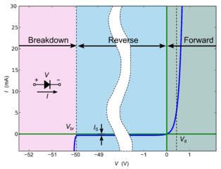
Diodes are really great! In a simple sense, they can give you a "point of no return" in your circuit (but they can actually do much more than that). Three interesting things should be observed from the IV characteristic shown to the right:
- For small positive voltages and above, the diode does not limit the current (the line is almost vertical)!
- For small to larger negative voltages, the diode resists current (the line is almost flat).
- For a large negative voltage (the breakdown voltage) the diode gives up (no one is perfect).
We can formally define this line with the Shockley Diode Equation, which formalizes this observation:
[math]\displaystyle{ I = I_S \left( e^{\frac{V_D}{n V_T}} - 1 \right) }[/math] where
[math]\displaystyle{ I }[/math] is the diode current,
[math]\displaystyle{ I_S }[/math] is the reverse bias saturation current (or scale current),
[math]\displaystyle{ V_D }[/math] is the voltage across the diode,
[math]\displaystyle{ V_T }[/math] is the thermal voltage, and
[math]\displaystyle{ n }[/math] is the ideality factor, (1 if the diode is ideal, greater than 1 if it is imperfect).
A great practical use for diodes is a rectifier:

This makes sure that when a positive voltage appears on either line, it is redirected to a single positive line, and the same for the negatives. BAM! AC to DC, that's pretty easy, you can charge your phone with that. In reality a capacitor is added in parallel with the load to try to smooth out the ripples. A voltage regulator after the rectifying step is also a popular choice, depending on the needs of the application.
Another super useful application is that of a back up power supply: simply connect two supplies in parallel with the positive terminals buffered with diodes. The higher of the two voltages is always used and the transition between supplies is seamless.
Zener Diodes
Some diodes (Zener) are made to have small breakdown voltages. Since during breakdown the IV curve is almost vertical (it's really an exponential), the current is independent (almost) from voltage. You can then wire up a Zener diode in reverse to a point in the circuit, and it will accept as much current as it needs to to reach that breakdown voltage. Because of this a great practical use for Zener diodes is a voltage regulator since the voltage is set when the diode is manufactured and does not change greatly with a varying power supply.
Bipolar Junction Transistors


Shortly after the invention of the first transistor (which was OK), the BJT landed, which was the first transistor to be prolific in the field.
It was made using two alternating NP junctions as shown below:

Really transistors (and by extension all that is needed for a computer to be built) are amplifiers (OK, to build all computers you need an inverting amplifier, but one can be built using the BJT). If one is used to thinking of them as an electrically-controlled switch, you can simply think of a switch as an amplifier with a gain of [math]\displaystyle{ \infty }[/math].
A simple model of a BJT is a linear current-controlled current source, i.e. the base to emitter (B to E) current [math]\displaystyle{ I_{BE} }[/math] is proportional to the collector to emitter (C to E) current [math]\displaystyle{ I_{CE} }[/math]. The proportionality constant [math]\displaystyle{ \beta }[/math] can be thought of as the "gain" of the transistor. This gives a relationship of [math]\displaystyle{ I_{CE} = \beta I_{BE} }[/math].

Sadly there is no source of infinite power, so the output to our amplifier tops off when it can't supply any more power. This can be seen with the graph on the right. The simple model then only works for the tiny linear part at the start of the graph, even so its not that linear. The BJT proved to be power hungry, pretty non-linear and sensitive to the environment (temperature, etc.). These growing pains lead to a new development, called the MOSFET.
MOSFETs
MOSFETs are the coolest, they are less power-hungy and easier to work with when compared to BJTs. Instead of having a current control, which uses power and gets the control and the output signal coupled together, a MOSFET's output is controlled by the electric Field (the F in MOSFET) the control signal creates on one of the plates of the MOSFET. Since the control signal and the output are electrically disconnected (as you would see in a capacitor) there is much less power draw from this type of transistor.
We can see how linear this thing is with its IV characteristic: [math]\displaystyle{ I_D= \mu_n C_{ox}\frac{W}{L} \left( (V_{GS}-V_{th})V_{DS}-\frac{V_{DS}^2}{2} \right) }[/math]
Apart from the control signal [math]\displaystyle{ V_{DS} }[/math] and constants, the voltage across the output portion of the MOSFET is linearly related to the current! This means that the MOSFET behaves like a voltage controlled resistor, and a resistor is something much easier to analyse and work with.
Most circuits with an enormous amount of transistors these days use primarily MOSFETs. BJTs are still useful for temperature and light sensing applications.
Industrial Semiconductor Fabrication
Semiconductors are mass produced in specialized factories called foundries or fabs. The process consists of multiple chemical and photolithographic steps which add layers to a wafer usually made of silicon. The entire process usually takes around 2 months but it can last up to 4.
The semiconductor product is rated by the size of the chip's process gate length, where processes with smaller gate lengths are typically harder to make. There are 10-20 different sized chips being fabricated around the world as of 2018. There is an immense amount of attention and money being dedicated to improving semiconductor fabrication process efficiency.

Examples
Simple
A simple application of a semiconductor would be the Cat's Whisker detector for radios, invented in the early 1900s.
Moderate
Optical sensors are moderately difficult applications of semiconductors. Optical sensors are electronic detectors that convert light into an electronic signal. They are used in many industrial and consumer applications. An example would include lamps that turn on automatically in response to darkness.
Difficult
A very complicated application of a semiconductor is its use in modern cellular phone devices, such as its use here in the iPhone 6.
See also
Related Wiki pages:
-Transformers
-Resistors and conductivity
-Superconductors
-Electric Fields
-Transformers from a physics standpoint
Further reading
Chabay, Sherwood. (n.d.). Matter and Interactions (4th ed., Vol. 2). Raleigh, North Carolina: Wiley.
Sze, S. (1981). Physics of semiconductor devices (2nd ed.). New York: Wiley.
External links
Wikipedia page about semiconductors:
https://en.wikipedia.org/wiki/Semiconductor_device
Encyclopedia entry about semiconductors, including the history of semiconductors:
http://www.britannica.com/technology/semiconductor-device
Information about Diodes:
https://en.wikipedia.org/wiki/Diode
Information about BJTs:
https://en.wikipedia.org/wiki/Bipolar_junction_transistor
Information about MOSFETs:
https://en.wikipedia.org/wiki/MOSFET
Semiconductor Device Fabrication
https://en.wikipedia.org/wiki/Semiconductor_device_fabrication
References
Brain, Marshall. "How Semiconductors Work." HowStuffWorks. N.p., 25 Apr. 2001. Web. 27 Nov. 2016.
Chabay, Sherwood. (n.d.). Matter and Interactions (4th ed., Vol. 2). Raleigh, North Carolina: Wiley.
Electronics and Semiconductor. (n.d.). Retrieved December 3, 2015, from http://www.plm.automation.siemens.com/en_us/electronics-semiconductor/devices/
Huculak, M. (2014, September 19). IPhone 6 and iPhone 6 Plus get teardown by iFixit • The Windows Site for Enthusiasts - Pureinfotech. Retrieved December 3, 2015, from http://pureinfotech.com/2014/09/19/iphone-6-iphone-6-plus-get-teardown-ifixit/
Introduction to Secondary Ion Mass Spectrometry (SIMS) technique. (n.d.). Retrieved November 15, 2020, from https://www.cameca.com/products/sims/technique
John Bardeen, William Shockley and Walter Brattain at Bell Labs, 1948. (n.d.). Retrieved December 3, 2015, from https://en.wikipedia.org/wiki/John_Bardeen#/media/File:Bardeen_Shockley_Brattain_1948.JPG
The Nobel Prize in Physics 1956. NobelPrize.org. Nobel Media AB 2018. Sun. 25 Nov 2018. <https://www.nobelprize.org/prizes/physics/1956/summary/>
The Nobel Prize in Physics 2000. NobelPrize.org. Nobel Media AB 2018. Sun. 25 Nov 2018. <https://www.nobelprize.org/prizes/physics/2000/summary/>
เซ็นเซอร์แสง (Optical Sensor) - Elec-Za.com. (2014, July 28). Retrieved December 3, 2015, from http://www.elec-za.com/เซ็นเซอร์แสง-optical-sensor/
Semiconductor device. (2015, November 30). Retrieved December 3, 2015, from https://en.wikipedia.org/wiki/Semiconductor_device
Semiconductor Fabrication. (25 November 2018). http://www.iue.tuwien.ac.at/phd/rovitto/node10.html
Shah, A. (2013, May 13). Intel loses ground as world's top semiconductor company, survey says. Retrieved December 3, 2015, from http://www.pcworld.com/article/2038645/intel-loses-ground-as-worlds-top-semiconductor-company-survey-says.html
Shaw, R. (2014, November 1). The cat's-whisker detector. Retrieved December 3, 2015, from http://rileyjshaw.com/blog/the-cat's-whisker-detector/
Sze, S. (2015, October 1). Semiconductor device | electronics. Retrieved December 3, 2015, from http://www.britannica.com/technology/semiconductor-device
Sze, S. (1981). Physics of semiconductor devices (2nd ed.). New York: Wiley.
"Timeline." Timeline | The Silicon Engine | Computer History Museum. The Silicon Engine, n.d. Web. 27 Nov. 2016.


